1
Æ
FN3980.15
HIN202, HIN206, HIN207, HIN208, HIN211, HIN213
+5V Powered RS-232
Transmitters/Receivers with
0.1Microfarad External Capacitors
The HIN202, HIN206, HIN207, HIN208, HIN211, HIN213
family of RS-232 transmitters/receivers interface circuits
meet all ElA RS-232E and V.28 specifications, and are
particularly suited for those applications where
±
12V is not
available. They require a single +5V power supply and
feature onboard charge pump voltage converters which
generate +10V and -10V supplies from the 5V supply The
family of devices offers a wide variety of RS-232
transmitter/receiver combinations to accommodate various
applications (see Selection Table).
The HIN206, HIN211 and HIN213 feature a low power
shutdown mode to conserve energy in battery powered
applications. In addition, the HIN213 provides two active
receivers in shutdown mode allowing for easy "wakeup"
capability.
The drivers feature true TTL/CMOS input compatibility, slew
rate-limited output, and 300
power-off source impedance.
The receivers can handle up to
±
30V input, and have a 3k
to 7k
input impedance. The receivers also feature
hysteresis to greatly improve noise rejection.
Applications
∑ Any System Requiring RS-232 Communications Port
- Computer - Portable, Mainframe, Laptop
- Peripheral - Printers and Terminals
- Instrumentation
- Modems
Features
∑ Meets All RS-232E and V.28 Specifications
∑ Requires Only 0.1
µ
F or Greater External Capacitors
∑ High Data Rate. . . . . . . . . . . . . . . . . . . . . . . . . . .120kbit/s
∑ Two Receivers Active in Shutdown Mode (HIN213)
∑ Requires Only Single +5V Power Supply
∑ Onboard Voltage Doubler/Inverter
∑ Low Power Consumption (Typ) . . . . . . . . . . . . . . . . . 5mA
∑ Low Power Shutdown Function (Typ) . . . . . . . . . . . . .1
µ
A
∑ Three-State TTL/CMOS Receiver Outputs
∑ Multiple Drivers
-
±
10V Output Swing for +5V lnput
- 300
Power-Off Source Impedance
- Output Current Limiting
- TTL/CMOS Compatible
- 30V/
µ
s Maximum Slew Rate
∑ Multiple Receivers
-
±
30V Input Voltage Range
- 3k
to 7k
Input Impedance
- 0.5V Hysteresis to Improve Noise Rejection
Selection Table
PART
NUMBER
POWER SUPPLY
VOLTAGE
NUMBER OF
RS-232
DRIVERS
NUMBER OF
RS-232
RECEIVERS
NUMBER OF
0.1
µ
F
EXTERNAL
CAPACITORS
LOW POWER
SHUTDOWN/TTL
THREE-STATE
NUMBER OF
RECEIVERS
ACTIVE IN
SHUTDOWN
HIN202
+5V
2
2
4 Capacitors
No/No
0
HIN206
+5V
4
3
4 Capacitors
Yes/Yes
0
HIN207
+5V
5
3
4 Capacitors
No/No
0
HIN208
5V
4
4
4 Capacitors
No/No
0
HIN211
+5V
4
5
4 Capacitors
Yes/Yes
0
HIN213
+5V
4
5
4 Capacitors
Yes/Yes
2
Data Sheet
September 2003
CAUTION: These devices are sensitive to electrostatic discharge; follow proper IC Handling Procedures.
1-888-INTERSIL or 321-724-7143
|
Intersil (and design) is a registered trademark of Intersil Americas Inc.
Copyright © Intersil Americas Inc. 2003. All Rights Reserved.
All other trademarks mentioned are the property of their respective owners.

2
Ordering Information
PART NO.
TEMP.
RANGE (
o
C)
PACKAGE
PKG.
DWG. #
HIN202CB
0 to 70
16 Ld SOIC (W)
M16.3
HIN202CB-T
0 to 70
16 Ld SOIC (W)
Tape and Reel
M16.3
HIN202CBN
0 to 70
16 Ld SOIC (N)
M16.15
HIN202CBN-T
0 to 70
16 Ld SOIC (N)
Tape and Reel
M16.15
HIN202CP
0 to 70
16 Ld PDIP
E16.3
HIN202IB
-40 to 85
16 Ld SOIC (W)
M16.3
HIN202IBN
-40 to 85
16 Ld SOIC (N)
M16.15
HIN206CB
0 to 70
24 Ld SOIC
M24.3
HIN207CA
0 to 70
24 Ld SSOP
M24.209
HIN207CB
0 to 70
24 Ld SOIC
M24.3
HIN207CB-T
0 to 70
24 Ld SOIC
Tape and Reel
M24.3
HIN208CB
0 to 70
24 Ld SOIC
M24.3
HIN208CB-T
0 to 70
24 Ld SOIC
Tape and Reel
M24.3
HIN211CA
0 to 70
28 Ld SSOP
M28.209
HIN211CA-T
0 to 70
28 Ld SSOP
Tape and Reel
M28.209
HIN211CB
0 to 70
28 Ld SOIC
M28.3
HIN211CB-T
0 to 70
28 Ld SOIC
Tape and Reel
M28.3
HIN213CA
0 to 70
28 Ld SSOP
M28.209
HIN213CA-T
0 to 70
28 Ld SSOP
Tape and Reel
M28.209
Ordering Information
(Continued)
PART NO.
TEMP.
RANGE (
o
C)
PACKAGE
PKG.
DWG. #
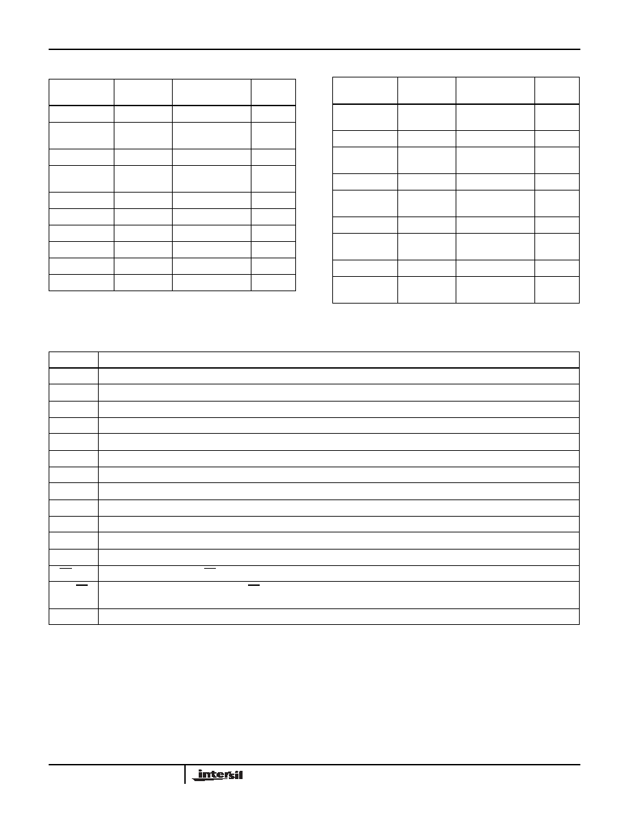
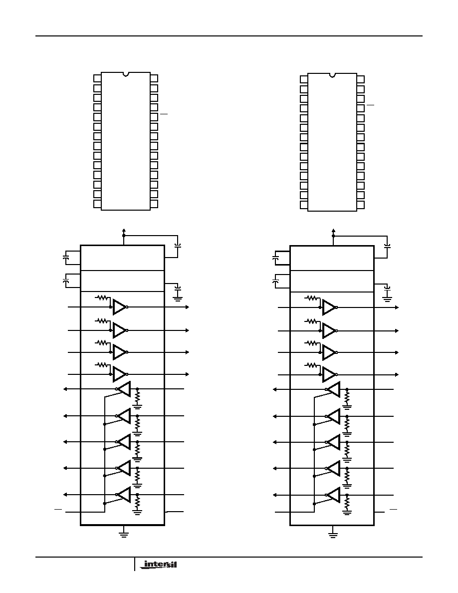
Pin Descriptions
PIN
FUNCTION
V
CC
Power Supply Input 5V
±
10%, (5V
±
5% HIN207).
V+
Internally generated positive supply (+10V nominal).
V-
Internally generated negative supply (-10V nominal).
GND
Ground Lead. Connect to 0V.
C1+
External capacitor (+ terminal) is connected to this lead.
C1-
External capacitor (- terminal) is connected to this lead.
C2+
External capacitor (+ terminal) is connected to this lead.
C2-
External capacitor (- terminal) is connected to this lead.
T
IN
Transmitter Inputs. These leads accept TTL/CMOS levels. An internal 400k
pull-up resistor to V
CC
is connected to each lead.
T
OUT
Transmitter Outputs. These are RS-232 levels (nominally
±
10V).
R
IN
Receiver Inputs. These inputs accept RS-232 input levels. An internal 5k
pull-down resistor to GND is connected to each input.
R
OUT
Receiver Outputs. These are TTL/CMOS levels.
EN, EN
Receiver enable Input. With EN = 5V (HIN213 EN = 0V), the receiver outputs are placed in a high impedance state.
SD, SD
Shutdown Input. With SD = 5V (HIN213 SD = 0V), the charge pump is disabled, the receiver outputs are in a high impedance state
(except R4 and R5 of HIN213) and the transmitters are shut off.
NC
No Connect. No connections are made to these leads.
HIN202, HIN206, HIN207, HIN208, HIN211, HIN213
